Also known as:
- VPL VPL201
Description:
VL82C311 SCAMP-DT
Versions:
- VL82C311-FC unknown MHz max
- VL82C311-25FC 25 MHz
- VL82C311-33FC4 33 MHz
The VL82C311, is a Single Chip AT, Mid-range Performance (SCAMP) Controllers for 286- or 386SX-based PC/AT compatible systems.
The VL82C311 includes the dual 82C37 DMA controllers, dual 82C59A programmable interrupt controllers, 82C54 programmable inter- val timer, 82284 clock and ready generator, 82288 bus controller and the logic for address/data bus control, memory control, shut down, refresh generation and refresh/DMA arbitration.
The VL82C311 is designed to perform in 386SX- based PC/AT-compatible systems running up to 25 MHz.
The memory controller logic is capable of accessing up to 16 MB of on-board DRAM. There can be up to four banks of 256K, 1M, or 4M in the system. The SCAMP Controller can drive four banks without external buffering. Built-in Page Mode operation and two-way interleaving allow the PC designer to maximize system performance using low-cost DRAMs. Zero and one wait state operation of system DRAM is supported.
There are 36 Mapping Registers in the SCAMP Controller for full EMS 4.0 standard. The system allows backfill down to 256K for EMS and provides 24 mapping registers covering this space. All registers are capable of translating over the complete range of on-board DRAM. Users can disable the on-board EMS system as well as system board DRAM.
The SCAMP handles system board refresh directly and controls the timing of slot bus refresh. Refresh is performed synchronously. Refreshes are staggered to minimize power supply loading and attenuate noise. Refresh can be programmed to support CAS-before-RAS refresh operation or standard RAS-only refresh operation. The SCAMP supports the PC/AT standard refresh period of 15.625 us as well as 125 us.
The VL82C311 has eight Mapping Registers to support 32 MB of JEIDA IC Memory Card, also known as PC Card.
The 287 coprocessor is supported when the SCAMP Controller is strapped for 286 Mode. When configured for 386SX Mode, the 387SX is supported.
The interrupt controller logic consists of two 82C59 megacells which are cascaded internally allowing a total of 13 external interrupt requests. There is a special programmable logic included in the SCAMP Controller which allows glitch-free inputs on all the interrupt request pins.
The counter/timer has three independent 16-bit counters and six programmable counter modes.
The DMA controllers are 82C37 compatible. DMA can transfer data over the full 16 MB range available. 74LS612 memory mappers are integrated provided to generate the upper address bits.
The SCAMP can be programmed for asynchronous or synchronous operation of the AT bus.
The SCAMP also performs all the data buffer control functions required for a 386SX based PC/AT system. Under the control of the CPU, the SCAMP routes data to and from the CPU's D bus, the internal XD bus, and the slots (SD bus). The parity is checked for D bus DRAM read operations. The data is latched for synchronization with the CPU. Parity is generated for all data written to the D bus.
Features:
- Fully compatible with 286- or 386SX-based PC/AT compatible systems (VL82C311L is 286 compatible only)
- Up to 25 MHz system clock in a 386SX-based system and up to 20 MHz in a 286-based system
- Replaces the following peripheral logic on the motherboard:
- Two 82C37A DMA controllers
- 74LS612 memory mapper
- Two 82C59A interrupt controllers
- 82C54 timer
- 82284 clock generator and ready interface
- 82288 bus controller
- Includes:
- Memory/refresh controller
- Port B, and NMI logic
- Bus steering logic
- Parity generation logic
- Parity checking logic
- Turbo control logic
- Staggered refresh to minimize power supply load variations
- Three-state control pin for board level testing
- Memory controller features include:
- Programmable option for page mode or non-page mode operation
- Two-way block interleaving
- Programmable option for zero and one wait state operation
- Capability to drive up to four banks directly
- Supports:
- Up to 16 MB system memory
- LIM EMS 4.0 over entire system memory
- VL82C325 (SX) Cache controller
- Four 16-bit wide banks of 256K, 1M, or 4M DRAM or SRAM
- Shadow RAM in 640K to 1M range
- 287 and 387SX numeric coprocessors
- 8- and 16-bit wide BIOS ROMs
- Asynchronous slot bus operation
- Systems with up to 16 MHz backplane operation
- Relocation of video and slot ROMs
- Other advanced features:
- Programmable I/O decode for 10- pr 16-bit addresses
- Hardware configurable setup to minimize custom BIOS requirements
- Programmable drive current to reduce ringing on DRAM and slot bus interface signals
- Programmable, extendable peripheral cycle
- Capability to disable software coprocessor reset
- Automatic bus speed-up on video access
- 1.0-micron CMOS technology
- 160-lead metric quad flat pack (MQFP)
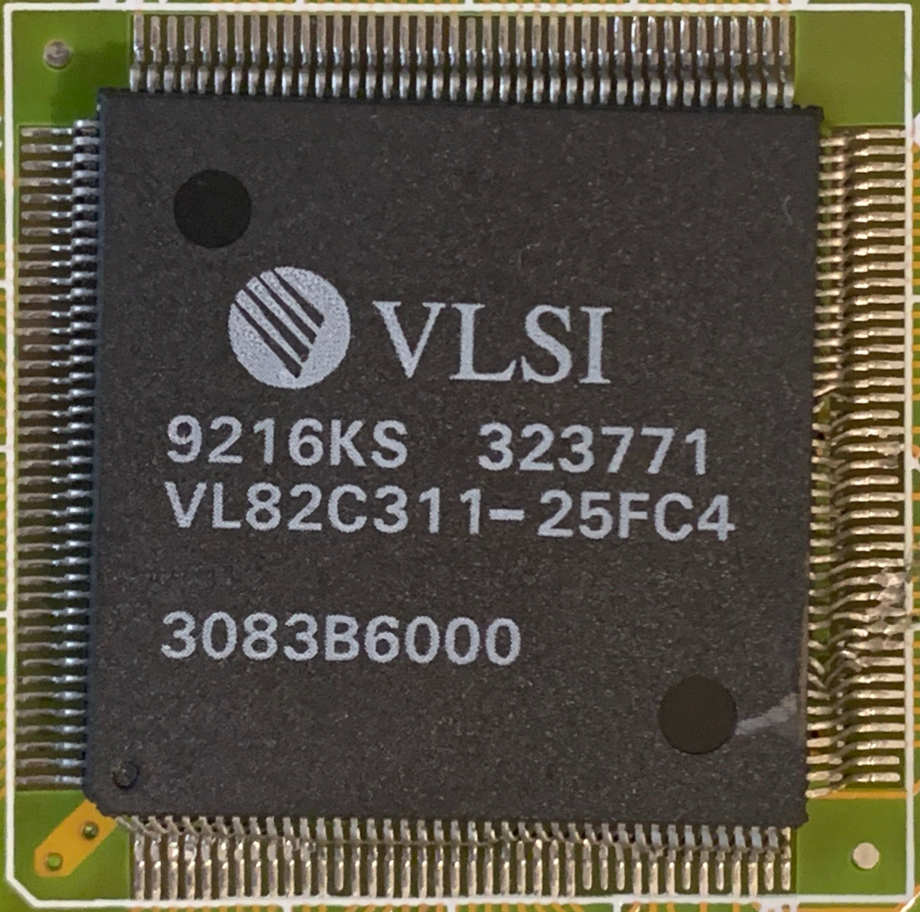 Image 1 of 2 (RetroShare)
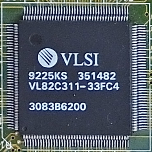 Image 2 of 2 (Rigo "0xCats" Reddig)
Disclaimer
The info found in this page might not be entirely correct. Check out this guide to learn how you can improve it.