VIA VT82C598MVP (VIA MVP3)
Chipset part
1106
Empty
Also known as:
- PCChips H.T.82C598AT (PC100 AGPro)
Description:
Overview
The VIA Apollo MVP3 aka VT82C598MVP/VT82C598AT is a Single-Chip Socket-7 / Super-7 North Bridge for Desktop and Mobile PC Systems with AGP and PCI plus Advanced ECC Memory Controller supporting SDRAM, EDO, and FPG ram.
Features
WIP
-
Interfaces
- AGP / PCI / ISA / ISA Mobile
- Single chip implementation for 64-bit Socket-7-CPU Host Bus, 64-bit system memory, 32-bit PCI and 32-bit AGP interfaces
- Supports 3.3V and sub-3.3V interface to CPU
- Supports separately powered 3.3V (5V tolerant) interface to system memory, AGP, and PCI bus
- PC-97 compatible using VIA VT82C586B (208-pin PQFP) south bridge chip with ACPI Power Management
- Modular power management and clock control for mobile system applications
-
Integration
- VT82C598MVP system controller with PCI link to VT82C586B PCI to ISA bridge
- VT82C586B also includes UltraDMA-33 EIDE, USB, and Keyboard / PS2-Mouse Interfaces plus RTC / CMOS on chip
- Can be combined with VIA VT82C596 (Intel PIIX4 pin compatible 324-pin BGA) “Mobile South” south bridge chip
-
CPU Interface
- Supports all Socket-7 processors including 64-bit Intel Pentium / Pentium with MMX, AMD K6, Cyrix/IBM 6X86 / 6X86MX, and IDT/Centaur C6 CPUs
- 66 / 75 / 83 / 100 MHz CPU external bus speed (internal 300MHz and above)
- Built-in deskew DLL (Delay Lock Loop) circuitry for optimal skew control within and between clocking regions
- Cyrix/IBM 6X86 linear burst support
- AMD K6 write allocation support
- System management interrupt, memory remap and STPCLK mechanism
-
Advanced Cache Controller
- Direct map write back or write through secondary cache
- Pipelined burst synchronous SRAM (PBSRAM) cache support
- Flexible cache size: 0K / 256K / 512K / 1M / 2MB
- 32 byte line size to match the primary cache
- Integrated 8-bit tag comparator
- 3-1-1-1-1-1-1-1 back to back read timing for PBSRAM access up to 100 MHz
- Tag timing optimized (less than 4ns setup time) to allow external tag SRAM implementation for most flexible cache organization
- Sustained 3 cycle write access for PBSRAM access or CPU to DRAM & PCI bus post write buffers up to 100 MHz
- Supports CPU single read cycle L2 allocation
- System and video BIOS cacheable and write-protect
- Programmable cacheable region
Last updated 2024-04-18T17:11:23Z
No chip specs
Name
Version
OS support
Size
Filename
Name
Version
4.35V
OS support
Size
973.7KB
Filename
Release date
File
Logs
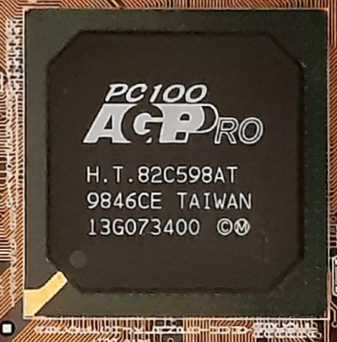 Image 1 of 2 (Carlos S. M.)
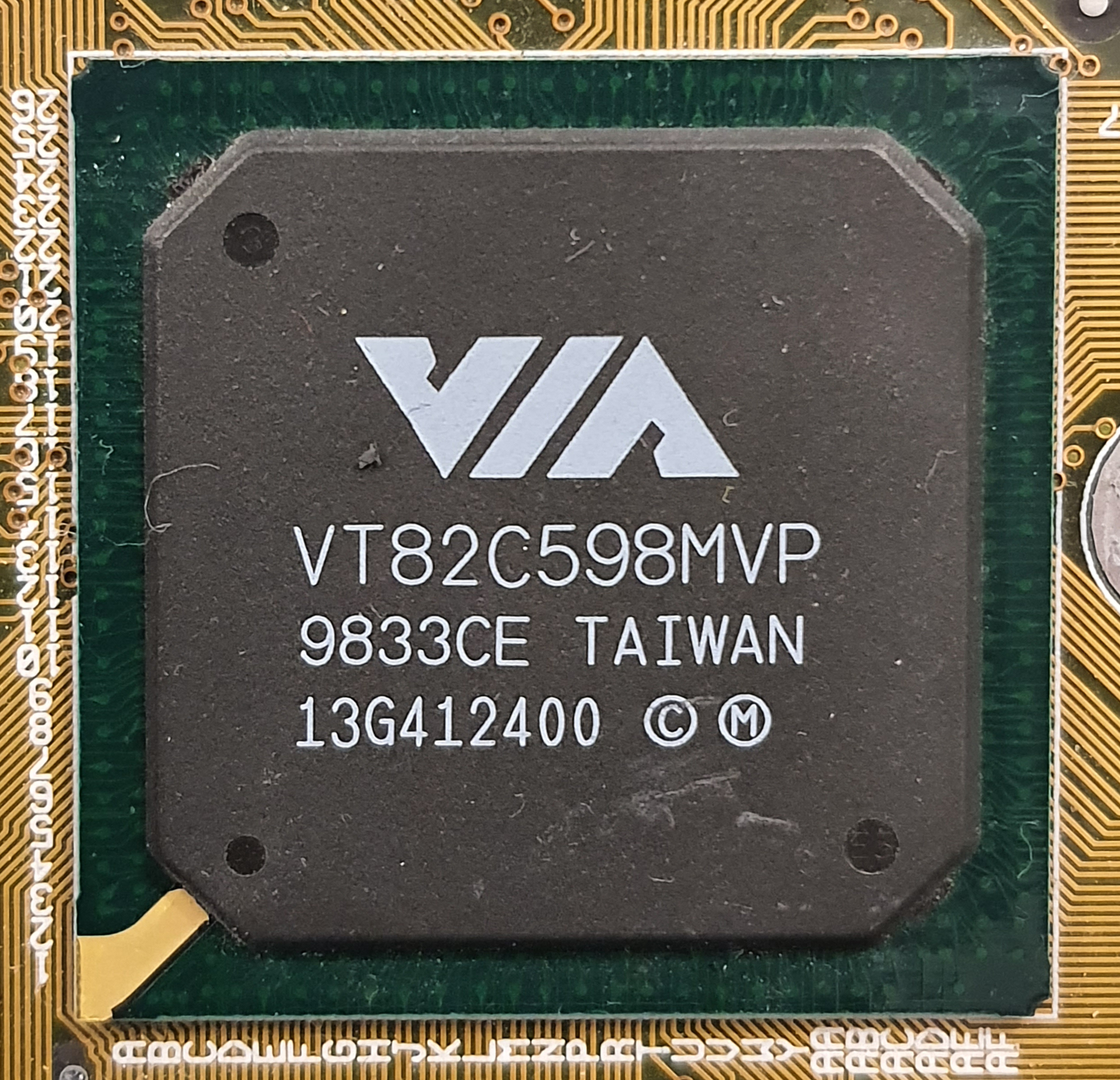 Image 2 of 2 (computerguy096)
Disclaimer
The info found in this page might not be entirely correct. Check out this guide to learn how you can improve it.